EZMod3D is a division of EASii IC, which develops a 3D multi-domain physical simulation software solution (also called 3D field solver) mainly developed to process the design of integrated circuits (ASICs), printed circuit boards (PCBs) and both at the same time (CoDesign).
EZMod3D was developed on the basis of an innovative solver enabling a fast simulation. This technology has allowed intensive use internally at EASii IC, targeting the requirements of our project: reducing iterations between design and manufacturing.
Nowadays, the importance of pre-sizing is becoming paramount.
- Reduce development costs based on accurate and fast 3D simulations
- Optimize time to market, using EZMod3D from the pre-dimensioning phase to manufacturing
- Allow and strengthen the collaborative work of your designers
- Educational approach, simulate physics easily and assess the impact on your designs yourself
- Low investment and attractive pricing
For all the engineers designing :
- Integrated (ASIC Designers, Physical designers, ...)
- Packaging (PCB, ASIC Designers & Co Design specialists, ...)
- Printed circuit boards ( CAD division, ... )
- Complex Systems (Data transmission systems, Cooling system, ...)
In your ASIC:
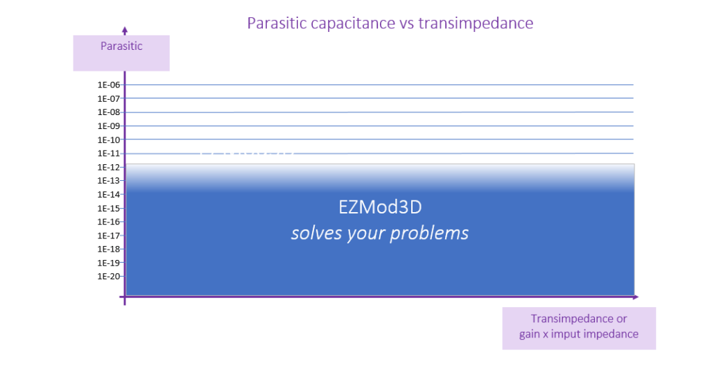
- Do you have frequencies or more broadly with a high band gain product?
- Do you have high currents or more broadly high power?
- Do you have converters with more than 10 bit resolution?
- Do you have mixed circuits (analog / digital) with power supply (IR DROP) or partitioning problems?
- Do you have substrate couplings, parasite through the dielectric, temperature sensitivity, etc.) ?
On your board :
- Do you encounter stability problems (oscillations on signals)?
- Are you worried about overheating or do you simply have thermal constraint ?
- Does your board embed relatively large size, a very large number of layers and vias?
- Does your power supply need to be analyzed and protected?
- What is the ASIC / PCB coupling from a capacitive or thermal point of view?
Considering your package :
- Which heat dissipation strategy to choose?
- Constrained environments where the packaging is problematic?
- What types of package, dimensions and materials?
- What is the ASIC / Package and Package / PCB interaction from a capacitive or thermal point of view?
Very simple, you just need to start with your input data
- The GDS2 file, OASIS database, LEF / DEF (ASIC) or Gerber (PCB) or DXF (Packaging)
- Technological file or materials description
- The position of the potentials or flows to be applied
In pre-sizing step, you can sketchup thanks to advanced user intergrated matrial library
Depending on the type of Physical Simulation you want to simulate, you will get for:
- Thermal simulation
Temperature mapping also including visualization of the gradient, Power flux, Thermal conductivity
- Electrical simulation
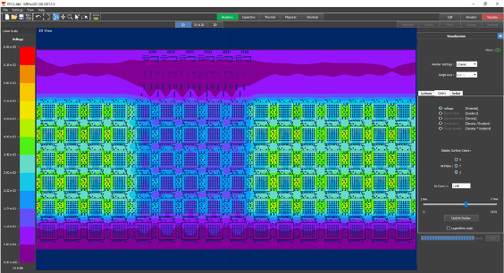
Potential mapping, Current density, Gradient, … and the SPICE Netlist
- Magnetic simulation
Magnetic Field Strengh, H-B Field visualization, … and the SPICE Netlist
- Electrostatic simulation:
Potential mapping, Electric field… and the SPICE Netlist
Please find below some EZMod3D examples regarding your job : ASIC, PCB, Packaging or System
Set your Example:
In a recent IC design, we had to use separate masses between the upper level blocks and separate the substrate from the masses.
Anytime an IC substrate is not connected to ground, there may be a problem with ESD protection.
In order to respond to this problem, we have chosen to use a pair of back-to-back protection diodes between each mass and between the substrate and each mass.
With extremely low resistance and inductance to the PCB, this will provide both ESD protection and acceptable insulation.
The example is a four stage op amp based amplifier with significant gain (> 80 dB) and moderate bandwidth (10 MHz).
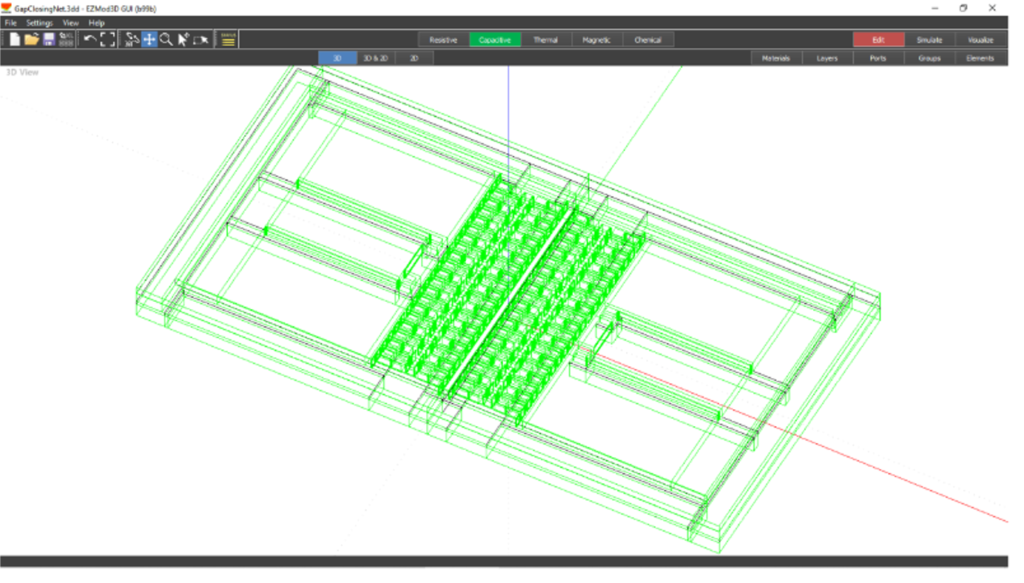
The addition of parasitic caps (105 capacities …) causes a strong peak in the frequency response which does not exist without parasitic caps
It’s not so easy to find the thermal resistance of that transistor attached to the bottom of the chip, but it’s even harder to find out how quickly the device heats up when the energy is dissipated inside.
EZMod3D can not only extract the thermal resistance but also the thermal behavior of the device on the frequency which is related to its dynamic behavior.
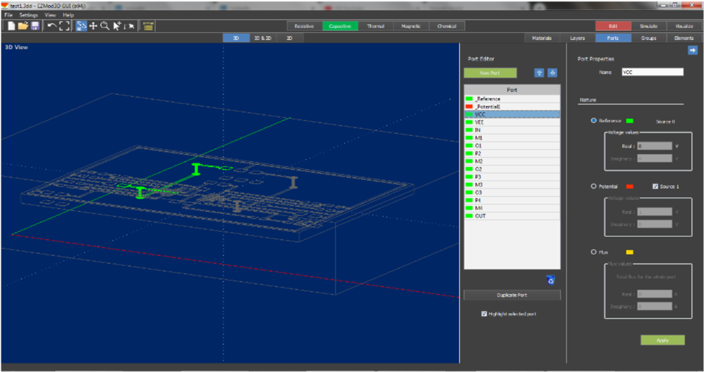
Consider the power supply of 256 asics.
The voltage drops for large currents will greatly influence the proper functioning of your card.
The question also is to know where to connect the regulator in order to compensate for all the problems of voltage drop.
In electronic systems and devices, parasitic elements are becoming more and more critical: The integration and density of the board reduce the distance between the components, increasing the unexpected / unwanted interactions.
Parasite elements can lead to non-functional designs and often impair design performance.
Parasitic elements are found in the layout of integrated circuits, but also in the casing and in the printed circuits around integrated circuits: the extraction of parasites must cover the whole range of design.
Thus, high performance applications require precise modeling of parasitic elements.
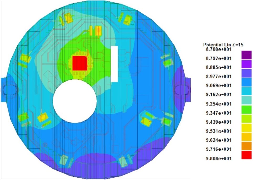
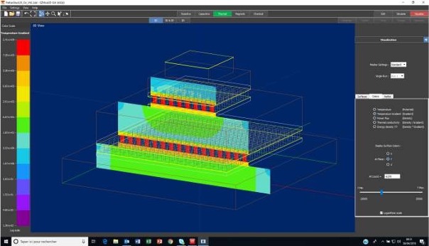
Show an overview of the temperature distribution of an LED bulb with driver on a PCB?
From the stacked files, the data was imported into EZMod3D, in thermal mode.
Then, the data of the PCB substrate was collected from the manufacturer.
This substrate is aluminum-ceramic with traces of copper on the top.
The power dissipated values in the driver IC and in each LED have been collected and added in EZMod3D as power sources.
As regards the layout of the printed circuits, the width of the tracks is generally chosen for the series resistance and / or for the current density.
In a number of cases, the current flowing in the tracks is not pure direct current but can have a significant high frequency content.
This is the case in the SMPS design.
In which cases, minimization of the track inductance can be important?
The question is therefore: for a given track width, what factors can influence the inductance?
What happens when a device in an integrated circuit dissipates power?
What is the temperature of this device?
How fast does it heat up?
How does this affect devices in the neighborhood?
If you have ever been faced with these questions, you know how difficult it is to answer without building the experience.
EZMod3D provides a powerful and extremely cost effective answer to all of these questions.
Not only does it provide the solution in steady state, but it can also provide frequency domain analysis.
It is then possible to plot a frequency dependent temperature map or extract the heat transfer function from the power source to the temperature at any point!
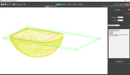
The example opposite shows a silicon chip inside a mini SO8 package.
A device, the small yellow rectangle, dissipates the power while the cold source, the large green square, is placed under the pads of the solder areas.
When it comes to MEMS design, everyone thinks of mechanical design and modeling tools and they are really needed.
But because a MEMS has an interface with an electronic circuit to condition the signals to a usable date, an electrical model is also needed to allow the design team to simulate the sensor with the conditioning IC.
Many MEMS sensors are of the capacitive type, that is to say they translate what they measure into variations in capacitance.
The interface IC is basically a capacitance meter.
A capacitive MEMS not only exhibits one or more active capacitance values, those which change with the measured physical size, but also parasitic capacitance values which can reduce the effective sensitivity.
Opposite, here is the development of a system with an IR image sensor to be kept cool in a hot environment with predefined mechanical constraints.
The goal is to properly size Peltier modules and stacking hardware to meet dissipation requirements before building a prototype.
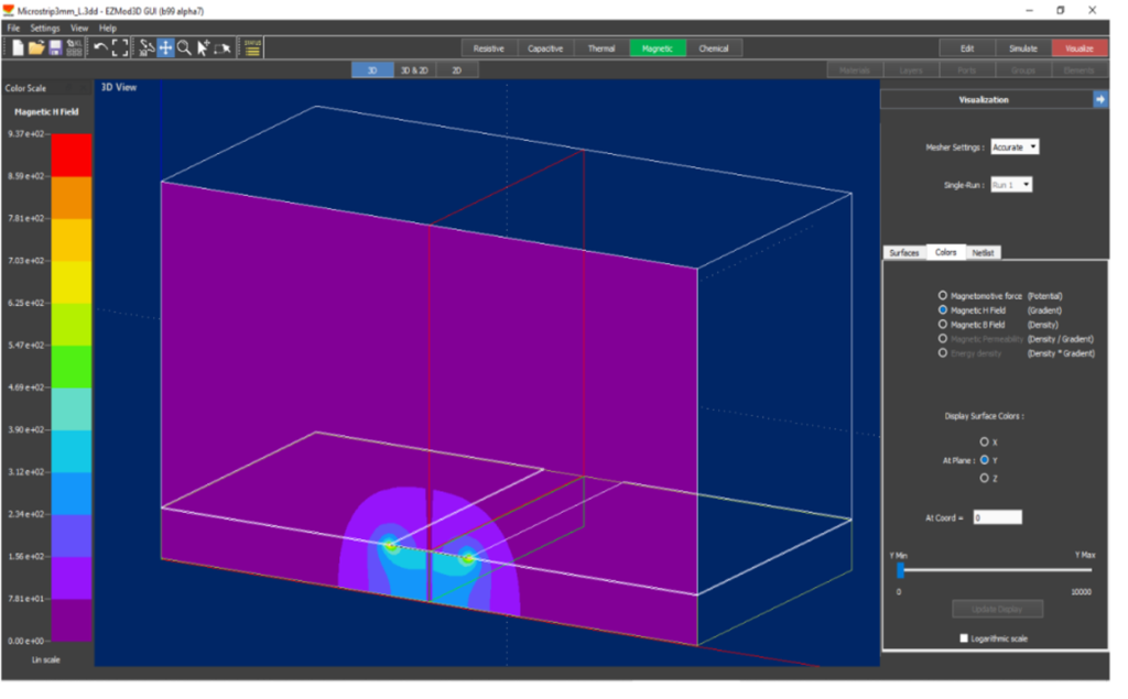
If you’ve ever wondered how a ferrite bead increases wire inductance, here’s a short review that might help.
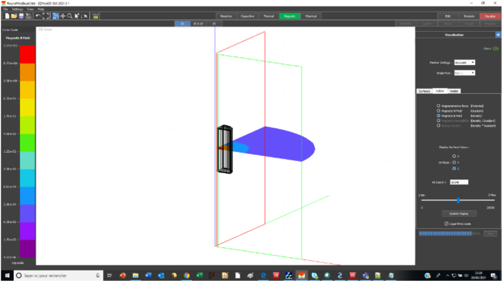
We use EZMod3D in the magnetic field and we show the effect of the ferrite bead on the reluctance then the inductance.
Consider a straight round wire. Thanks to symmetry, we can only simulate a quarter of the section of the wire. In order for the magnetic field to extend around the wire, we need to define a surrounding airspace. Now, as everyone knows, the magnetic field revolves around the wire and decreases by 1 / distance as Ampere’s theorem says.
And at high frequencies where most of the current flows on the surface of the conductor, the same theorem shows that there is no magnetic flux inside the conductor.
Fill out the form below and receive by email the link to download the installation pack
